🚚 Free Worldwide Shipping on All Orders!Shop Now
A11051 - SN74LS221N Dual Monostable Multivibrators (TI)
The SN74LS221N devices are monolithic dual multivibrators with performance characteristics virtually identical to those of the '121 devices. Each multivibrator features a negative-transition- triggered input and a positive-transition-triggered input, either of which can be used as an inhibit input. Pulse triggering occurs at a particular voltage level and is not directly related to the transition time of the input pulse. Schmitt-trigger input circuitry (TTL hysteresis) for B input allows jitter-free triggering from inputs with transition rates as slow as 1 V/s, providing the circuit with excellent noise immunity, typically of 1.2 V. A high immunity to VCC noise, typically of 1.5 V, is also provided by internal latching circuitry.
Once fired, the outputs are independent of further transitions of the A and B inputs and are a function of the timing components, or the output pulses can be terminated by the overriding clear. Input pulses can be of any duration relative to the output pulse. Output pulse length can be varied from 35 ns to the maximums shown in the above table by choosing appropriate timing components. With Rext = 2 k Ohm and Cext = 0, an output pulse typically of 30 ns is achieved, which can be used as a dc-triggered reset signal. Output rise and fall times are TTL compatible and independent of pulse length. Typical triggering and clearing sequences are shown as a part of the switching characteristics waveforms.
Pulse-width stability is achieved through internal compensation and is virtually independent of VCC and temperature. In most applications, pulse stability is limited only by the accuracy of external timing components. Jitter-free operation is maintained over the full temperature and VCC ranges for more than six decades of timing capacitance (10 pF to 10 ?F) and more than one decade of timing resistance (2 k Ohm to 100 k Ohm). Throughout this range, pulse width is defined by the relationship: tw(out) = CextRext In2 0.7 CextRext. In circuits where pulse cutoff is not critical, timing capacitance up to 1000 ?F and timing resistance as low as 1.4 k Ohm can be used. Also, the range of jitter-free output pulse widths is extended if VCC is held to 5 V and free-air temperature is 25?C. Duty cycles as high as 90% are achieved when using maximum recommended RT. Higher duty cycles are available if a certain amount of pulse-width jitter is allowed.
Features:
Overriding Clear Terminates Output Pulse
Datasheet Available:Texas Instruements SN74LS221N
16 pin DIP. Manufactured by Texas Instruments.
A11051
$0.14
Original: $0.40
-65%A11051 - SN74LS221N Dual Monostable Multivibrators (TI)—
$0.40
$0.14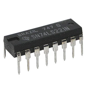
Description
The SN74LS221N devices are monolithic dual multivibrators with performance characteristics virtually identical to those of the '121 devices. Each multivibrator features a negative-transition- triggered input and a positive-transition-triggered input, either of which can be used as an inhibit input. Pulse triggering occurs at a particular voltage level and is not directly related to the transition time of the input pulse. Schmitt-trigger input circuitry (TTL hysteresis) for B input allows jitter-free triggering from inputs with transition rates as slow as 1 V/s, providing the circuit with excellent noise immunity, typically of 1.2 V. A high immunity to VCC noise, typically of 1.5 V, is also provided by internal latching circuitry.
Once fired, the outputs are independent of further transitions of the A and B inputs and are a function of the timing components, or the output pulses can be terminated by the overriding clear. Input pulses can be of any duration relative to the output pulse. Output pulse length can be varied from 35 ns to the maximums shown in the above table by choosing appropriate timing components. With Rext = 2 k Ohm and Cext = 0, an output pulse typically of 30 ns is achieved, which can be used as a dc-triggered reset signal. Output rise and fall times are TTL compatible and independent of pulse length. Typical triggering and clearing sequences are shown as a part of the switching characteristics waveforms.
Pulse-width stability is achieved through internal compensation and is virtually independent of VCC and temperature. In most applications, pulse stability is limited only by the accuracy of external timing components. Jitter-free operation is maintained over the full temperature and VCC ranges for more than six decades of timing capacitance (10 pF to 10 ?F) and more than one decade of timing resistance (2 k Ohm to 100 k Ohm). Throughout this range, pulse width is defined by the relationship: tw(out) = CextRext In2 0.7 CextRext. In circuits where pulse cutoff is not critical, timing capacitance up to 1000 ?F and timing resistance as low as 1.4 k Ohm can be used. Also, the range of jitter-free output pulse widths is extended if VCC is held to 5 V and free-air temperature is 25?C. Duty cycles as high as 90% are achieved when using maximum recommended RT. Higher duty cycles are available if a certain amount of pulse-width jitter is allowed.
Features:
Overriding Clear Terminates Output Pulse
Datasheet Available:Texas Instruements SN74LS221N
16 pin DIP. Manufactured by Texas Instruments.
A11051
Once fired, the outputs are independent of further transitions of the A and B inputs and are a function of the timing components, or the output pulses can be terminated by the overriding clear. Input pulses can be of any duration relative to the output pulse. Output pulse length can be varied from 35 ns to the maximums shown in the above table by choosing appropriate timing components. With Rext = 2 k Ohm and Cext = 0, an output pulse typically of 30 ns is achieved, which can be used as a dc-triggered reset signal. Output rise and fall times are TTL compatible and independent of pulse length. Typical triggering and clearing sequences are shown as a part of the switching characteristics waveforms.
Pulse-width stability is achieved through internal compensation and is virtually independent of VCC and temperature. In most applications, pulse stability is limited only by the accuracy of external timing components. Jitter-free operation is maintained over the full temperature and VCC ranges for more than six decades of timing capacitance (10 pF to 10 ?F) and more than one decade of timing resistance (2 k Ohm to 100 k Ohm). Throughout this range, pulse width is defined by the relationship: tw(out) = CextRext In2 0.7 CextRext. In circuits where pulse cutoff is not critical, timing capacitance up to 1000 ?F and timing resistance as low as 1.4 k Ohm can be used. Also, the range of jitter-free output pulse widths is extended if VCC is held to 5 V and free-air temperature is 25?C. Duty cycles as high as 90% are achieved when using maximum recommended RT. Higher duty cycles are available if a certain amount of pulse-width jitter is allowed.
Features:
Overriding Clear Terminates Output Pulse
Datasheet Available:Texas Instruements SN74LS221N
16 pin DIP. Manufactured by Texas Instruments.
A11051