🚚 Free Worldwide Shipping on All Orders!Shop Now
A20244S - SN74LVCH16244ADGGR SMD 16-Bit Buffer/Driver (TI)
This 16-bit buffer/driver is designed for 1.65-V to 3.6-V VCC operation. The SN74LVCH16244ADGGR is designed specifically to improve the performance and density of 3-state memory address drivers, clock drivers, and bus-oriented receivers and transmitters. The device can be used as four 4-bit buffers, two 8-bit buffers, or one 16-bit buffer. It provides true outputs and symmetrical active-low output-enable (OE) inputs. To ensure the high-impedance state during power up or power down, OE should be tied to VCC through a pullup resistor; the minimum value of the resistor is determined by the current-sinking capability of the driver. Inputs can be driven from either 3.3-V or 5-V devices. This feature allows the use of this device as a translator in a mixed 3.3-V/5-V system environment. This device is fully specified for partial-power-down applications using Ioff. The Ioff circuitry disables the outputs, preventing damaging current backflow through the device when it is powered down. Active bus-hold circuitry holds unused or undriven inputs at a valid logic state. Use of pullup or pulldown resistors with the bus-hold circuitry is not recommended.
Features:
Operates From 1.65 V to 3.6 V
Inputs Accept Voltages to 5.5 V
Max tpd of 4.1 ns at 3.3 V
Typical VOLP (Output Ground Bounce) < 0.8 V at VCC = 3.3 V, TA = 25?C
Typical VOHV (Output VOH Undershoot) >2 V at VCC = 3.3 V, TA = 25?C
Ioff Supports Partial-Power-Down Mode Operation
Supports Mixed-Mode Signal Operation on All Ports (5-V Input/Output Voltage With 3.3-V VCC)
Bus Hold on Data Inputs Eliminates the Need for External Pullup/Pulldown Resistors
Datasheet Available:Texas Instruments SN74LVCH16244ADGGR
TSSOP-48 package. Manufactured by Texas Instruments.
A20244S
$0.31
Original: $0.89
-65%A20244S - SN74LVCH16244ADGGR SMD 16-Bit Buffer/Driver (TI)—
$0.89
$0.31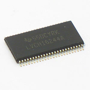
Description
This 16-bit buffer/driver is designed for 1.65-V to 3.6-V VCC operation. The SN74LVCH16244ADGGR is designed specifically to improve the performance and density of 3-state memory address drivers, clock drivers, and bus-oriented receivers and transmitters. The device can be used as four 4-bit buffers, two 8-bit buffers, or one 16-bit buffer. It provides true outputs and symmetrical active-low output-enable (OE) inputs. To ensure the high-impedance state during power up or power down, OE should be tied to VCC through a pullup resistor; the minimum value of the resistor is determined by the current-sinking capability of the driver. Inputs can be driven from either 3.3-V or 5-V devices. This feature allows the use of this device as a translator in a mixed 3.3-V/5-V system environment. This device is fully specified for partial-power-down applications using Ioff. The Ioff circuitry disables the outputs, preventing damaging current backflow through the device when it is powered down. Active bus-hold circuitry holds unused or undriven inputs at a valid logic state. Use of pullup or pulldown resistors with the bus-hold circuitry is not recommended.
Features:
Operates From 1.65 V to 3.6 V
Inputs Accept Voltages to 5.5 V
Max tpd of 4.1 ns at 3.3 V
Typical VOLP (Output Ground Bounce) < 0.8 V at VCC = 3.3 V, TA = 25?C
Typical VOHV (Output VOH Undershoot) >2 V at VCC = 3.3 V, TA = 25?C
Ioff Supports Partial-Power-Down Mode Operation
Supports Mixed-Mode Signal Operation on All Ports (5-V Input/Output Voltage With 3.3-V VCC)
Bus Hold on Data Inputs Eliminates the Need for External Pullup/Pulldown Resistors
Datasheet Available:Texas Instruments SN74LVCH16244ADGGR
TSSOP-48 package. Manufactured by Texas Instruments.
A20244S
Features:
Operates From 1.65 V to 3.6 V
Inputs Accept Voltages to 5.5 V
Max tpd of 4.1 ns at 3.3 V
Typical VOLP (Output Ground Bounce) < 0.8 V at VCC = 3.3 V, TA = 25?C
Typical VOHV (Output VOH Undershoot) >2 V at VCC = 3.3 V, TA = 25?C
Ioff Supports Partial-Power-Down Mode Operation
Supports Mixed-Mode Signal Operation on All Ports (5-V Input/Output Voltage With 3.3-V VCC)
Bus Hold on Data Inputs Eliminates the Need for External Pullup/Pulldown Resistors
Datasheet Available:Texas Instruments SN74LVCH16244ADGGR
TSSOP-48 package. Manufactured by Texas Instruments.
A20244S