🚚 Free Worldwide Shipping on All Orders!Shop Now
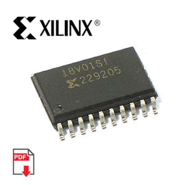
A20566S - XC18V01 SMD In-System Programmable Config PROM (Xilinx)
The XC18V01 is a in-system programmable configuration PROM. This 3.3V PROM provides an easy-to-use method for re-programming and storing large Xilinx FPGA or CPLD configuration bitstreams. When the FPGA is in Master Serial mode, it generates a configuration clock that drives the PROM. A short access time after the rising CCLK, data is available on the PROM DATA (D0) pin that is connected to the FPGA DIN pin. The FPGA generates the appropriate number of clock pulses to complete the configuration. When the FPGA is in Slave Serial mode, the PROM and the FPGA are clocked by an external clock.
When the FPGA is in Slave-Parallel or SelectMAP Mode, an external oscillator generates the configuration clock that drives the PROM and the FPGA. After the rising CCLK edge, data are available on the PROMs DATA (D0-D7) pins. The data is clocked into the FPGA on the following rising edge of the CCLK. Neither Slave-Parallel nor SelectMAP utilize a Length Count, so a free-running oscillator can be used. Multiple devices can be concatenated by using the CEO output to drive the CE input of the following device. The clock inputs and the DATA outputs of all PROMs in this chain are interconnected. The XC18V01S020I is compatible andcan be cascaded with other members of the XC18V00 Series family or with the XC17V00 one-time programmable Serial PROM family. The XC18V01S020I has a guaranteed endurance level of 20,000 in-system program/erase cycles and a minimum data retention of 20 years.
Features:
In-system programmable 3.3V PROM for configuration of Xilinx FPGAs
- Endurance of 20,000 program/erase cycles
- Program/erase over full industrial voltage and temperature range
Simple interface to the FPGA
Cascadable for storing longer or multiple bitstreams
Low-power advanced CMOS FLASH process
Dual configuration modes
- Serial Slow/Fast configuration (up to 33 MHz)
- Parallel (up to 264 Mb/s at 33 MHz)
5V tolerant I/O pins accept 5V, 3.3V and 2.5V signals
3.3V or 2.5V output capability
SOIC 20 package. Manufactured by Xilinx.
A20566S
| Additional Resources |
$3.95
A20566S - XC18V01 SMD In-System Programmable Config PROM (Xilinx)—
$3.95
Description
The XC18V01 is a in-system programmable configuration PROM. This 3.3V PROM provides an easy-to-use method for re-programming and storing large Xilinx FPGA or CPLD configuration bitstreams. When the FPGA is in Master Serial mode, it generates a configuration clock that drives the PROM. A short access time after the rising CCLK, data is available on the PROM DATA (D0) pin that is connected to the FPGA DIN pin. The FPGA generates the appropriate number of clock pulses to complete the configuration. When the FPGA is in Slave Serial mode, the PROM and the FPGA are clocked by an external clock.
When the FPGA is in Slave-Parallel or SelectMAP Mode, an external oscillator generates the configuration clock that drives the PROM and the FPGA. After the rising CCLK edge, data are available on the PROMs DATA (D0-D7) pins. The data is clocked into the FPGA on the following rising edge of the CCLK. Neither Slave-Parallel nor SelectMAP utilize a Length Count, so a free-running oscillator can be used. Multiple devices can be concatenated by using the CEO output to drive the CE input of the following device. The clock inputs and the DATA outputs of all PROMs in this chain are interconnected. The XC18V01S020I is compatible andcan be cascaded with other members of the XC18V00 Series family or with the XC17V00 one-time programmable Serial PROM family. The XC18V01S020I has a guaranteed endurance level of 20,000 in-system program/erase cycles and a minimum data retention of 20 years.
Features:
In-system programmable 3.3V PROM for configuration of Xilinx FPGAs
- Endurance of 20,000 program/erase cycles
- Program/erase over full industrial voltage and temperature range
Simple interface to the FPGA
Cascadable for storing longer or multiple bitstreams
Low-power advanced CMOS FLASH process
Dual configuration modes
- Serial Slow/Fast configuration (up to 33 MHz)
- Parallel (up to 264 Mb/s at 33 MHz)
5V tolerant I/O pins accept 5V, 3.3V and 2.5V signals
3.3V or 2.5V output capability
SOIC 20 package. Manufactured by Xilinx.
A20566S
When the FPGA is in Slave-Parallel or SelectMAP Mode, an external oscillator generates the configuration clock that drives the PROM and the FPGA. After the rising CCLK edge, data are available on the PROMs DATA (D0-D7) pins. The data is clocked into the FPGA on the following rising edge of the CCLK. Neither Slave-Parallel nor SelectMAP utilize a Length Count, so a free-running oscillator can be used. Multiple devices can be concatenated by using the CEO output to drive the CE input of the following device. The clock inputs and the DATA outputs of all PROMs in this chain are interconnected. The XC18V01S020I is compatible andcan be cascaded with other members of the XC18V00 Series family or with the XC17V00 one-time programmable Serial PROM family. The XC18V01S020I has a guaranteed endurance level of 20,000 in-system program/erase cycles and a minimum data retention of 20 years.
Features:
In-system programmable 3.3V PROM for configuration of Xilinx FPGAs
- Endurance of 20,000 program/erase cycles
- Program/erase over full industrial voltage and temperature range
Simple interface to the FPGA
Cascadable for storing longer or multiple bitstreams
Low-power advanced CMOS FLASH process
Dual configuration modes
- Serial Slow/Fast configuration (up to 33 MHz)
- Parallel (up to 264 Mb/s at 33 MHz)
5V tolerant I/O pins accept 5V, 3.3V and 2.5V signals
3.3V or 2.5V output capability
SOIC 20 package. Manufactured by Xilinx.
A20566S
| Additional Resources |