🚚 Free Worldwide Shipping on All Orders!Shop Now
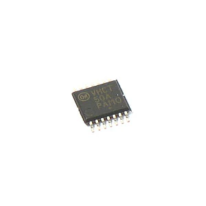
A20570S - MC74VHCT50ADTR2G SMD Buffer/CMOS Logic Lvl Shifter (On Semi)
The MC74VHCT50ADTR2G is a hex noninverting buffer fabricated with silicon gate CMOS technology. It achieves high speed operation similar to equivalent bipolar Schottky TTL while maintaining CMOS low power dissipation. The internal circuit is composed of three stages, including a buffered output which provides high noise immunity and stable output.
The device input is compatible with TTL-type input thresholds and the output has a full 5V CMOS level output swing. The input protection circuitry on this device allows overvoltage tolerance on the input, allowing the device to be used as a logic-level translator from 3.0V CMOS Logic while operating at the high-voltage power supply.
The MC74VHCT50ADTR2G input structure provides protection when voltages up to 7.0V are applied, regardless of the supply voltage. This allows the MC74VHCT50ADTR2G to be used to interface 5V circuits to 3V circuits. The output structures also provide protection when VCC = 0V. These input and output structures help prevent device destruction caused by supply voltage-input/output voltage mismatch, battery backup, hot insertion, etc.
Features:
High Speed: tPD = 3.5ns (Typ) at VCC = 5V
Low Power Dissipation: ICC = 2mA (Max) at TA = 25?C
TTL-Compatible Inputs: VIL = 0.8V; VIH = 2.0V
CMOS-Compatible Outputs: VOH > 0.8VCC; VOL < 0.1VCC @Load
Power Down Protection Provided on Inputs and Outputs
TSSOP 14 package. Manufactured by On Semi.
A20570S
| Additional Resources |
$0.25
A20570S - MC74VHCT50ADTR2G SMD Buffer/CMOS Logic Lvl Shifter (On Semi)—
$0.25
Description
The MC74VHCT50ADTR2G is a hex noninverting buffer fabricated with silicon gate CMOS technology. It achieves high speed operation similar to equivalent bipolar Schottky TTL while maintaining CMOS low power dissipation. The internal circuit is composed of three stages, including a buffered output which provides high noise immunity and stable output.
The device input is compatible with TTL-type input thresholds and the output has a full 5V CMOS level output swing. The input protection circuitry on this device allows overvoltage tolerance on the input, allowing the device to be used as a logic-level translator from 3.0V CMOS Logic while operating at the high-voltage power supply.
The MC74VHCT50ADTR2G input structure provides protection when voltages up to 7.0V are applied, regardless of the supply voltage. This allows the MC74VHCT50ADTR2G to be used to interface 5V circuits to 3V circuits. The output structures also provide protection when VCC = 0V. These input and output structures help prevent device destruction caused by supply voltage-input/output voltage mismatch, battery backup, hot insertion, etc.
Features:
High Speed: tPD = 3.5ns (Typ) at VCC = 5V
Low Power Dissipation: ICC = 2mA (Max) at TA = 25?C
TTL-Compatible Inputs: VIL = 0.8V; VIH = 2.0V
CMOS-Compatible Outputs: VOH > 0.8VCC; VOL < 0.1VCC @Load
Power Down Protection Provided on Inputs and Outputs
TSSOP 14 package. Manufactured by On Semi.
A20570S
The device input is compatible with TTL-type input thresholds and the output has a full 5V CMOS level output swing. The input protection circuitry on this device allows overvoltage tolerance on the input, allowing the device to be used as a logic-level translator from 3.0V CMOS Logic while operating at the high-voltage power supply.
The MC74VHCT50ADTR2G input structure provides protection when voltages up to 7.0V are applied, regardless of the supply voltage. This allows the MC74VHCT50ADTR2G to be used to interface 5V circuits to 3V circuits. The output structures also provide protection when VCC = 0V. These input and output structures help prevent device destruction caused by supply voltage-input/output voltage mismatch, battery backup, hot insertion, etc.
Features:
High Speed: tPD = 3.5ns (Typ) at VCC = 5V
Low Power Dissipation: ICC = 2mA (Max) at TA = 25?C
TTL-Compatible Inputs: VIL = 0.8V; VIH = 2.0V
CMOS-Compatible Outputs: VOH > 0.8VCC; VOL < 0.1VCC @Load
Power Down Protection Provided on Inputs and Outputs
TSSOP 14 package. Manufactured by On Semi.
A20570S
| Additional Resources |